# CL_DRAM_DMA CustomLogic Example
## :exclamation: NOTE: If this is your first time using F1, you should read [How To Create an Amazon FPGA Image (AFI) From One of The CL Examples: Step-by-Step Guide](./../../../../README.md) first!!
## Table of Content
1. [Overview](#overview)
2. [Functional Description of the example RTL](#functionalDescription)
3. [Software](#software)
4. [DRAM DMA Example Metadata](#metadata)
# Overview
The CL_DRAM_DMA example demonstrates the use and connectivity for many of the Shell/CL interfaces and functionality, including:
1) Register Access over ocl\_ AXI-Lite interfaces
2) Mapping of the external four DRAM channel to instance memory via PCIe AppPF BAR4, and the 512-bit pcis_dma_ AXI4 bus
3) Virtual JTAG and Xilinx Integrated Logic Analyzer cores
4) User-defined interrupts
5) pcim_ AXI4 traffic for host memory accesses from CL
### System diagram
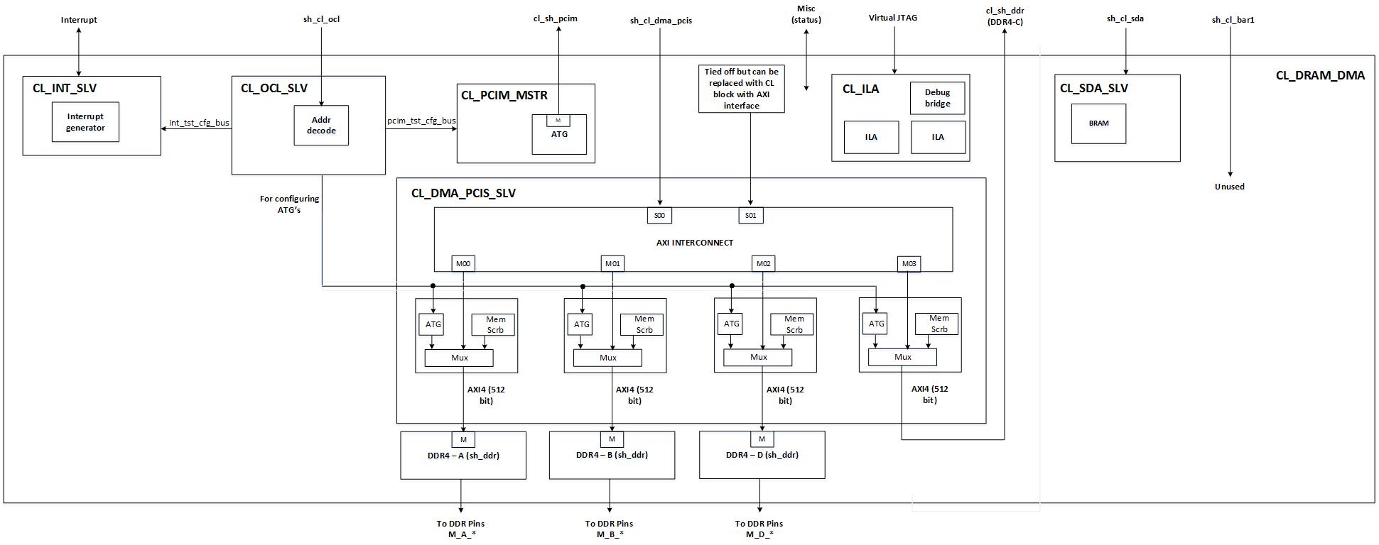
# Functional Description
### DRAM Interfaces
All four DRAM channels are used.
The DRAM space is 64GiB, and is mapped to the sh_cl_dma_pcis AXI4 bus.
### Disabling Unused DDR controllers for simulation
Disabling unused DDR controllers will improve simulation performance. cl_dram_dma example has all DDR controllers enabled by default. To disable a DDR controller which is not used follow the steps below.
#### Design Changes
Individual DDR controllers can be enabled and disabled by simply updating the appropriate defines in the [cl_dram_dma_defines.vh](design/cl_dram_dma_defines.vh) file. The [sh_ddr.sv](../../../common/shell_v04261818/design/sh_ddr/sim/sh_ddr.sv) file contains the necessary logic to remove and tie-off appropriate interfaces for the disabled DDR controllers.
For the cl_dram_dma example a memory range has been allocated for each DDR. So, if a particular DDR controller is disabled, then the developer should take care to handle transactions to that addresss range since there will be no DDR controller to respond to the request. The address ranges for each DDR controller is described below in the [dma_pcis AXI4 bus section](#dma_pcis).
#### Test Changes
If a particular ddr controller is disabled, make sure that the test is not accessing address space for that DDR controller.
Please look at [dma_pcis AXI4 bus section](#dma_pcis) for address ranges.
For DDRs that are enabled, make sure that the DDRs are initialized using the poke_stat commands below.
eg:
To initialize DDR_A, DDR-B and DDR-D
tb.poke_stat(.addr(8'h0c), .ddr_idx(0), .data(32'h0000_0000));
tb.poke_stat(.addr(8'h0c), .ddr_idx(1), .data(32'h0000_0000));
tb.poke_stat(.addr(8'h0c), .ddr_idx(3), .data(32'h0000_0000));
Make sure that the Host to Card and Card to Host DMA transfers only access enabled DDR controller address space.
### dma_pcis AXI4 bus
sh\_cl\_dma\_pcis exposes a address windows of 128GiB matching AppPF BAR4.
This memory space is mapped to the 64GiB DRAM space (the upper half of the 128GiB will just wrap around to the lower half).
An [axi_crossbar_0](../../../common/shell_v04261818/design/ip/cl_axi_interconnect/synth/cl_axi_interconnect.v)
will interleave inbound addresses according to DDR_A (base_addr=0x0_0000_00000, range=16GB),
DDR_B(base_addr=0x4_0000_0000, range=16GB), DDR_C(base_addr=0x8_0000_0000, range=16GB),
DDR_D(base_addr=0xC_0000_0000, range=16GB).
### ocl\_ AXI-Lite
The cl_ocl\_ AXI-Lite bus is connected to [cl_ocl_slv.sv](design/cl_ocl_slv.sv) module, and is used for register access to the Automatic Test Generator (ATG) etc.
The valid address map is found [cl_ocl_address_map.xlsx](design/address_map.xlsx).
Any access invalid address with return 32'hdeadbeef
### sda\_ AXI-Lite
The sh_cl_sda\_ AXI-Lite bus is connected to [cl_sda_slv.sv](design/cl_sda_slv.sv) module, which provides 1KiB of scratch RAM.
Address bits [9:0] will be used to access the location of the RAM, but the upper bits of the address are ignored.
### pcim\_ AXI4
The cl_sh_pcim\_ AXI4 bus is driven by Automatic Test Generator (ATG) and connected to [cl_pcim_mstr.sv](design/cl_pcim_mstr.sv). It can be used to read/write from the host memory.
### irq/ack
[cl_int_slv.sv](design/cl_int_slv.sv) provides an example for generating the IRQ requests and checks if ACK has been received.
### FPGA to FPGA communication over PCIe
This example does not use FPGA to FPGA PCIe communication
### FPGA to FPGA communication over Ring
This example does not use FPGA to FPGA Ring. FPGA Ring is a unsupported feature planned for future release.
### Virtual JTAG
2 ILA cores are integrated, one to monitoring the sh\_c_dma\_pcis bus and the other to monitor the AXI4 signals on DDR_A. An example usage is provided in [cl_ila.sv](design/cl_ila.sv).
An example usage for Xilinx VIO is provided in [cl_vio.sv](design/cl_vio.sv)
### Clocks
CL_DRAM_DMA uses the main `clk_main_a0`. It's frequency is set in the cl_clk under `build/constraints/cl_clocks.xdc`.
`clk_xtra_a1` is used by the Virtual JTAG
### Reset
flr_reset is ignored in this design
## Runtime software
DMA accesses rely on the [XDMA driver](../../../../sdk/linux_kernel_drivers/xdma/README.md)
Developers using AMI 1.5.0 or Later Instances that come with pre-installed Xilinx Runtime Environment (XRT) should [refer to this note](../../../../sdk/linux_kernel_drivers/xdma/xdma_install.md#xdmainstallfail) before installing the XDMA driver.
The DRAM DMA example includes runtime software to demonstrate working DMA accesses. The runtime example is located [in the runtime directory](software/runtime/test_dram_dma.c)
There are two example tests in cl_dram_dma example.
# test_dram_dma.c
This test runs a regular software test with data transfer with all 4 DMA channels enabled.
## Compile and run instructions
cd $CL_DIR/software/runtime
make all
sudo ./test_dram_dma
# test_dram_dma_hwsw_cosim.c
This test runs a software test with HW/SW co-simulation enabled with all 4 DMA channels enabled.
## Compile and run instructions
cd $CL_DIR/software/runtime
make TEST=test_dram_dma_hwsw_cosim
sudo ./test_dram_dma_hwsw_cosim
The test can be simulated with XSIM as follows.
cd $CL_DIR/verif/scripts
make C_TEST=test_dram_dma_hwsw_cosim
## DRAM DMA Example Metadata
The following table displays information about the CL that is required to register it as an AFI with AWS.
Alternatively, you can directly use a pre-generated AFI for this CL.
| Key | Value |
|-----------|------|
| Shell Version | 0x04261818 |
| PCI Device ID | 0xF001 |
| PCI Vendor ID | 0x1D0F (Amazon) |
| PCI Subsystem ID | 0x1D51 |
| PCI Subsystem Vendor ID | 0xFEDC |
| Pre-generated AFI ID | afi-063e6afe717a22158 |
| Pre-generated AGFI ID | agfi-0b5c35827af676702 |